Article Overview
Optical module packaging methods include COB, BOX, TO-CAN, and butterfly types, each designed to balance cost, reliability, heat dissipation, and environmental suitability.
Hermetic vs Non-Hermetic Packaging
Hermetic packaging involves sealing optical components in a protective enclosure, often filled with inert gas, to prevent moisture and dust ingress. This ensures high reliability and stable performance in harsh environments, such as outdoor telecom networks or industrial applications. Common hermetic packages include TO-CAN, BOX, and butterfly packages. Hermetic designs often incorporate thermoelectric coolers (TECs) for temperature-sensitive laser diodes, maintaining wavelength stability and device longevity . Non-hermetic packaging reduces cost and complexity by directly attaching optical chips to the PCB and sealing them with epoxy or adhesives. This approach, exemplified by Chip-on-Board (COB) packaging, is widely used in data centers and short-distance applications where environmental conditions are controlled .
Common Packaging Methods
1. Chip-on-Board (COB)
- Description: The laser or photodiode chip is mounted directly on the PCB.
- Advantages: Miniaturization, lightweight, lower cost, and shorter interconnection paths for improved performance.
- Applications: Data centers, high-performance computing, campus networks, and short-distance optical links.
- Limitations: Sensitive to environmental instability; not ideal for industrial or outdoor temperature extremes .
2. BOX Packaging
- Description: Optical components are enclosed in a metal box, often hermetically sealed with inert gas.
- Advantages: High reliability, stable optical and electrical performance, effective heat dissipation, and easier maintenance.
- Applications: Carrier-grade telecom modules, 100G optical transceivers, data centers, and high-performance computing networks.
- Characteristics: Suitable for harsh environments with large temperature and humidity fluctuations .
3. TO-CAN Packaging
- Description: The laser is mounted on a small heat sink and enclosed in a metal can with a sealed window.
- Advantages: Compact, cost-effective, and provides basic hermetic protection.
- Limitations: Limited volume restricts heat dissipation; not suitable for high-power or long-distance applications.
- Applications: Short to medium-distance telecom links, such as 10 km 10G/25G fronthaul and home broadband .
4. Butterfly Packaging
- Description: A specialized hermetic package often used for multi-channel transceivers.
- Advantages: Integrates multiple lasers in a single package, suitable for high-density, multi-channel applications.
- Applications: High-speed telecom and data center modules requiring precise temperature control and reliability .
Evolution and Trends
Optical module packaging has evolved from bulky GBIC modules to compact SFP, QSFP, QSFP-DD, and co-packaged optics (CPO). Miniaturization improves port density, reduces cost, and enhances performance for high-bandwidth applications like 5G, AI computing, and cloud storage . Modern packaging emphasizes integration, thermal management, and cost efficiency while maintaining optical alignment and reliability.
Key Considerations
- Environmental conditions: Hermetic packages for outdoor/industrial use; non-hermetic for controlled environments.
- Heat dissipation: BOX and TO-CAN packages often include heat sinks or thermal pads.
- Cost vs performance: COB reduces cost but may compromise environmental robustness; hermetic packages increase reliability at higher cost.
- Application distance: VCSEL chips in COB for short reach; DFB or EML chips in hermetic packages for medium to long distances . In summary, selecting an optical module packaging method requires balancing cost, reliability, thermal management, and environmental suitability, with COB, BOX, TO-CAN, and butterfly packages serving distinct roles across data center, telecom, and industrial applications.
Photonic Packaging – optical interfaces, package types, TO-can
Key optical interfacing methods are discussed, such as free-space optics, fiber-optic connections via edge coupling or grating
The Evolution of Optical Module Packaging From Bulky to Small
This article will use plain language to take you through the evolution of optical module packaging, and will also
Detailed Explanation of SFP Optical Module Packaging
The article details the packaging evolution, technical features (such as speed, compatibility, and modulation technology), and typical
Packaging Technologies for Optical Components: Integrated Module
The demands for high-speed data transmission and the needs for an integrated optical module comprising more functional optical
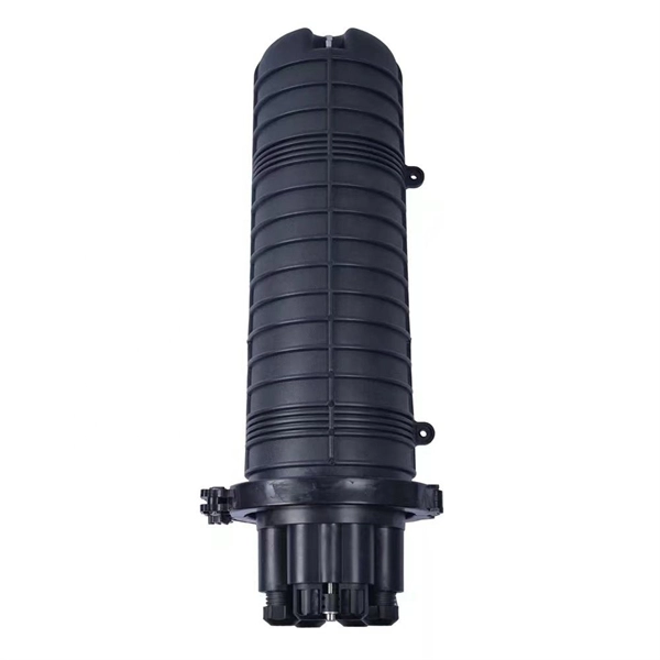
Four Optical Packaging Processes
Figure3: Optical receiving circuit schematic The basic structure of optical module package is Transmitting Optical Sub
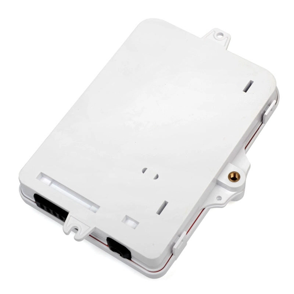
Optical module packaging form and size standards
Optical modules are an important part of optical communication systems and are used to transmit and receive optical
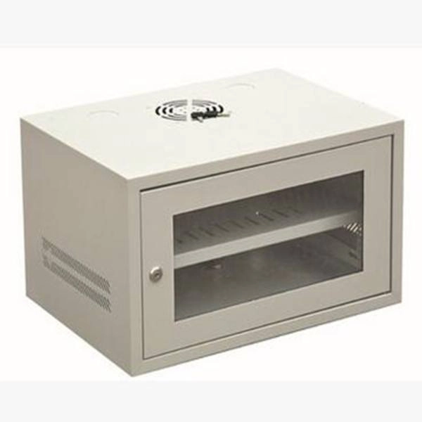
Design Guidelines for Photonic Integrated Circuit Packaging
Design Guidelines for Photonic Integrated Circuit Packaging PHIX is a one-stop-shop for the manufacturing of modules powered by
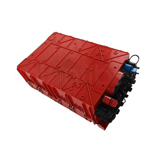
The Evolution of Optical Module Packaging From Bulky to Small
The packaging technology of optical modules is the "genetic code" that determines their performance, cost, and
Advanced Optical Integration Processes for Photonic‐Integrated
Next, we introduce photonic chip packaging methods applied to various optical devices at the chip level. Then, we
Optical Module: A Comprehensive Analysis from Source
NRZ modulation is a traditional optical module modulation method, and its principle is
Review of Packaging of Optoelectronic, Photonic, and MEMS Components
This paper reviews the packaging of optoelectronic, photonic, and microelectromechanical systems (MEMS)
Overview of Optical Module Modulation Technologies and Packaging
This article will delve into the current mainstream optical module modulation technologies, rates, and packaging types,
Module/packaging technologies for optical components: current and
The basic design methodology and criteria required for packaging of optical components are reviewed, and the state-of-art of
Optical Module Packaging: From Bulky Designs to SFP, QSFP, and
From the large GBIC in 1995 to today''s nano-scale QSFP-DD and co-packaged optics (CPO), how has packaging technology
Optical Transceiver: Packaging Methods & Optical Chip Types
This article analyzes the requirements of optical transceivers and discusses packaging methods and optical chip
LED and Optical Device Packaging and Materials
Abstract As for integrated circuit (IC) device packaging, the packaging materials are critical to the LED packaging because the device
Optical device packaging technology: COB,BOX and
In the field of optical communication,the packaging of optical devices plays a crucial role in
Advanced optical packaging – how much do you know ?
Regardless of the type of optical module, the production process generally consists of two
Understanding COB, BOX, and TO-CAN Packaging for Optical Devices
When it comes to optical devices, the right packaging technology can make all the difference. COB, BOX, and TO
Optical Packaging/Module Technologies: Design Methodologies
Achieving high performance in the module requires not only the chip design, but also requires the package design, which includes
Optical Packaging/Module Technologies | Request PDF
Achieving high performance in the module requires not only the chip design, but also requires the package design,
Four Optical Packaging Processes
FiberMall has a complete set of optical packaging technologies, which can be used for the development of each
Detailed Explanation of QSFP Optical Module Packaging
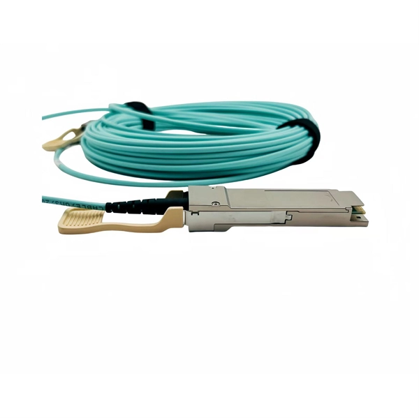
QSFP Package Fundamentals QSFP, short for Quad Small Form-factor Pluggable, is a four-channel small form-factor pluggable
Optical module – A comprehensive exploration
Traditional classification method: generally classified from the perspectives of packaging method, transmission rate,
Micro-Optical Packaging for High-Performance
Discover HOPP micro-optical packaging technology for ultra-compact optical modules with micron-level
Optical device packaging technology: COB,BOX and coaxial
Common optical device packaging methods include COB (chip-on-board packaging), BOX and coaxial packaging.
Advanced Optical Integration Processes for
First, we discuss the basic optical connection methods of PIC chips at the optical
TI DLP® System Design: Optical Module Specifications
ABSTRACT The objective of this application note is to help product developers better understand optical module specifications and
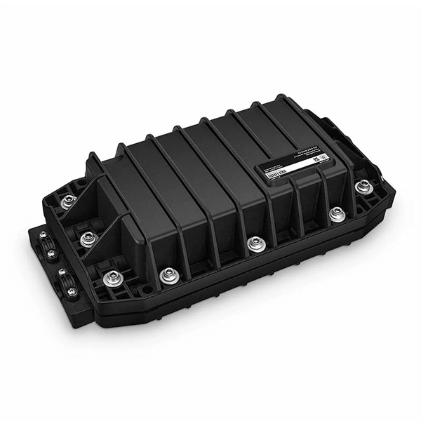
Opto-Electronic Packaging
„Opto-electronic packaging means working on the connection of opto-electronic integrated circuits to optical and electrical
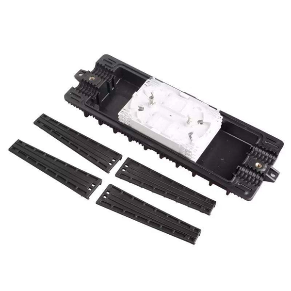
Optical Communication Module Chip Packaging | Weyland
Chip packaging design is a crucial factor that affects the performance, reliability, and thermal characteristics of optical
Related Resources
- Protection of underground optical cable junction boxes
- Communication Optical Cable Center Vertical Pipe
- Fiber Optic Connector Ceramic Flanger APC
- Classification of Relay Protection Maintenance
- Jamaica Professional Fireproof Cable Tray Price
- Tunisia Data Center Cable Management System Construction Case
- How to inspect a 48-port fiber optic patch panel